
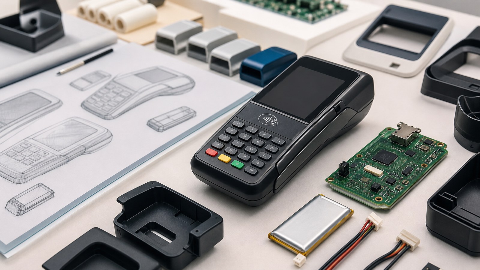
Start with the decisions that avoid late rework
One of the most common mistakes we see in custom POS device development is locking PCB layout or enclosure details before the payment and RF architecture are fixed. That drives late changes to the bill of materials, repeated RF tuning, and certification delays. A short, practical planning phase up front — focused on payment architecture, NFC/contactless and antenna choices, peripheral trade-offs, and a security-to-certification plan — reduces both technical risk and calendar slip.
Payment hardware architecture: pick the strategy that matches your roadmap
There are three pragmatic architecture patterns used in POS devices. Rather than a checklist-only exercise, match the pattern to your product lifecycle, certification tolerance, and volume targets.
A modular approach (application CPU plus a separate certified payment module or secure element) isolates payment scope, often shortening re-certification when your app layer changes. An integrated SoC design reduces BOM cost and enclosure size but increases integration work and can extend certification timelines because more of the stack is under your control. Many teams adopt a hybrid approach: a certified secure element or payment module for the sensitive path, and an application SoC for UI and connectivity to balance time-to-market and unit cost.
Decision drivers include expected product lifespan, planned field upgrades, target volumes, and who owns certification work. For example, if you anticipate frequent application updates or region-specific payment rules, a modular payment module can limit re-certification scope. If you are targeting very high volumes and want the lowest per-unit cost, integrated designs can make sense provided you budget the certification effort.
NFC and contactless: plan antenna and RF early
Contactless features are sensitive to mechanical layout. Choose whether to adopt a pre-certified NFC controller/module, pair it with a secure element, or design a deeper integrated RF path based on your certification strategy. Regardless, put antenna placement and tuning on the schedule before mechanical sign-off.
From a hands-on perspective, a few concrete considerations matter: keep the NFC antenna at least 8–12 mm from large ground planes or battery metal to avoid detuning; include a small ground cutout below the antenna region if the enclosure has metal parts; and provision a matching network pad or test connector on the PCB so the antenna can be tuned without re-spinning the full board. Antenna behavior also changes when the case material or thickness changes, so plan a mechanical/EM iteration early.
Finally, plan RF coexistence: Bluetooth, Wi‑Fi and cellular radios can interfere if antennas are poorly separated. A basic rule is to keep antenna-to-antenna spacing and to route RF ground consistently to reduce emissions and maintain read range.
Peripherals: printers, displays, and key input trade-offs
Peripheral choices strongly affect enclosure dimensions, power budget, and serviceability. Instead of long checklists, think in use-cases. A countertop terminal that prints receipts may prioritize an internal thermal printer and easy paper access; a handheld delivery unit will prioritize battery life, ruggedness, and a sealed keypad or full touchscreen. Indoor kiosks may use bright transmissive displays; outdoor or sunlight-exposed devices might need transflective or higher-brightness displays and anti-glare coatings.
Consider serviceability: positioning a thermal printer so it is user-serviceable reduces repair costs, but requires additional mechanical space and different EMI shielding choices versus a sealed, tamper-resistant design. Keypad style (mechanical keys vs. capacitive buttons) also affects sealing, tactile feedback, and EMI planning.
Example decision outcomes
| Use case | Architectural approach | Why |
|---|---|---|
| High-security countertop terminal | Modular payment module + SE | Limits PCI/EMV scope and simplifies re-certification for application updates |
| Low-cost indoor kiosk | Integrated SoC with basic NFC | Lower per-unit BOM at scale; plan for longer certification time |
| Handheld delivery POS | Rugged enclosure, antenna-optimized layout, battery-aware power design | Prioritize read range, thermal and mechanical resilience |
Security and certification planning: map the path early
Payment devices must follow applicable standards and the practical approach is to document scope early: which hardware and software elements fall under which standard, who owns evidence collection, and when lab testing happens in your schedule. Choosing a pre-certified payment module reduces your certification boundary, but you must preserve the module’s integrity across integration (secure boot, encrypted storage, tamper evidence). If you plan a full-board certification, include certification labs and timelines in your procurement and risk plan because test windows and required evidence change over time.
Sourcing, BOM and manufacturability: minimize surprises
Make BOM and sourcing decisions with alternate suppliers identified for long-lead or single-source parts. Decide early whether to use off-the-shelf modules (faster, lower technical risk) or custom boards/ASICs (lower unit cost at scale but higher NRE and time-to-market). For RF components and antennas, select vendors with POS experience and request reference samples early so you can validate performance in your enclosure.
Also plan for production test fixtures, firmware update paths, and spare-part strategies. These are frequently overlooked but are needed both for manufacturing acceptance and to provide certification evidence (for example, firmware version control and secure update logs).
Real-world scenarios (anonymized)
Scenario 1: A regional retailer chose an integrated SoC to hit a low-cost target. During enclosure finalization the NFC read range fell below spec because the battery and a metal holder were too close to the coil; the team needed two additional mechanical iterations and an antenna retune. Early antenna placement and a prototype antenna test cut that schedule cost in a later project.
Scenario 2: An outdoor kiosk project used a modular certified payment module to limit re-certification. That choice allowed the team to iterate on the application firmware and UI without repeating payment tests when the UI changed for different markets.
Implementation checklist before hardware design starts
- Finalize the payment architecture: modular, integrated, or hybrid, tied to your certification tolerance.
- Choose NFC/contactless controller approach and reserve antenna area with matching network access for tuning.
- Decide printer/display/keypad trade-offs with clear serviceability and power budgets.
- Create a security and design-to-certification plan that assigns responsibilities and milestones.
- Prepare a sourcing/BOM strategy with alternates, test-fixture plans, and long-lead items identified.
AI and advanced features: modern POS expectations
POS devices increasingly include AI-enabled features such as voice command interfaces, local predictive analytics for inventory or upsell suggestions, and secure on-device models. These introduce additional hardware choices (microphones array placement, on-device AI accelerators, low-latency memory) and privacy considerations. If you plan to include voice or edge inference, add those requirements to the architecture review so CPU, power, and thermal budgets account for on-device ML workloads.
FAQ
What are the first practical steps in custom POS device development?
Start with a short requirements workshop to decide payment architecture, NFC/contactless scope, and the peripheral set (printer/display/keypad). Add security and certification planning early, and capture these decisions in a one-page architecture summary that the mechanical, electrical and firmware teams can reference during design.
Should I use a certified payment module or integrate everything?
There is no universal right answer. A certified module reduces your certification surface and can speed time-to-market; integrating everything can be more cost-effective at high volumes but requires more integration and certification effort. Choose based on timeline, expected volumes, and whether you have the resources to manage full terminal certification.
How do I avoid NFC tuning issues late in the project?
Reserve the antenna area early, include a matching network and test points, and plan mechanical prototypes for antenna tuning. Keep the antenna away from large metal components and batteries where possible, and consider ferrite backing if the antenna must sit near metal. These steps let RF engineers tune the read range without multiple full-board spins.
Can Emszen help with custom POS device development and certification?
Yes. Emszen provides architecture reviews, prototype builds, BOM analysis, certification planning support, and access to a manufacturing partner network. We help scope integration vs. modular strategies, perform early RF/antenna assessments, and produce a certification roadmap you can present to labs and payment scheme partners. We provide guidance and deliverables but do not issue regulatory approvals; final certification must be completed by the designated test laboratories and issuing authorities.
Next step — a practical deliverable and how to contact Emszen
If you are planning custom POS device development, schedule a technical review with Emszen. We will produce an architecture review document that includes a recommended payment/SE approach, a BOM risk analysis, and a certification roadmap tailored to your markets. Contact Emszen through our website to request a technical review and receive a proposed scope and timeline for the deliverables.