
Antenna placement small electronics: Top mistakes
By Alex Chen, MSEE, RF systems engineer. 12 years in RF design, lead engineer on 20+ certified IoT products, and experienced with cellular, Wi Fi, and Bluetooth integration.
Early decisions about antenna integration determine whether a compact product passes certification and achieves reliable field performance. This article explains why antenna placement small electronics matters, the common placement mistakes we see, a decision framework to prioritize fixes, and concise testing steps to reduce rework during manufacturing. The guidance is conservative, and we recommend vendor or lab verification at each stage.
Why antenna placement small electronics matters
The physical constraints in compact devices change antenna impedance and radiation patterns. In small form factors, proximity to metal, ground plane geometry, and enclosure material can detune antennas and reduce link margin. These effects mean that antenna placement small electronics must be handled as a combined mechanical and RF design activity, not as an afterthought.
Common antenna placement mistakes and mitigations
Below are recurring errors we encounter on compact hardware projects, with practical mitigations you can apply during architecture and the first PCB revision.
- Metal obstruction: Antennas placed adjacent to metal brackets or shields suffer large efficiency loss. Mitigation: define no-metal keepout zones in mechanical drawings and plan antenna windows in the enclosure.
- Insufficient ground clearance: A truncated ground plane detunes many antenna types. Mitigation: specify minimum copper clearances, and include ground pour cutouts and test points for tuning.
- Hand and body effects: User grip detunes small antennas, affecting range and repeatability. Mitigation: prototype with representative grips and document user-hold guidance for the manual and packaging.
- Wrong enclosure material: Conductive fillers or metal coatings attenuate signals. Mitigation: test candidate plastics early or provide antenna windows, and consider external antennas where appropriate.
- Poor cable routing: Power and shielded cables routed across antenna zones cause coupling. Mitigation: lock down cable paths in assembly drawings and use clips to control movement.
- Coexistence issues: Poor separation between radios leads to packet loss and desensitization. Mitigation: plan filters, isolation, and minimum separation in the system architecture stage.
- Skipping matching footprints: Omitting tunable components increases spins. Mitigation: include matching network footprints and test points on the first PCB revision.
- Late RF review: Waiting until pre certification multiplies cost and schedule risk. Mitigation: schedule an RF review at schematic freeze and before tooling.
Testing and measurement best practices
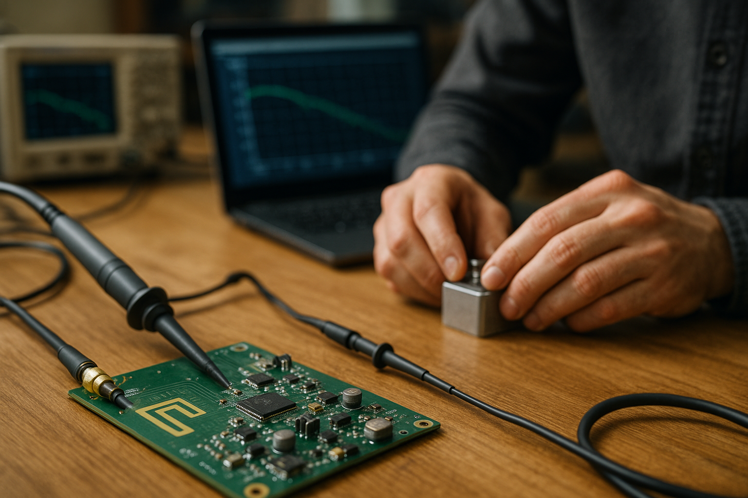
Testing early prevents surprises. When you measure, mimic production form factors, and use repeatable setups. Key steps:
- Prototype with final enclosure material or a calibrated dummy shell, so measurements reflect production behavior.
- Use a network analyzer early to validate matching networks, and check S11 across expected bands.
- Measure radiated performance in a semi anechoic chamber, or use calibrated near field probes if a chamber is not available.
- Test hand effects with standardized grips, and capture worst case orientations for product use cases.
For regulatory process details, refer to authoritative resources such as the FCC. See FCC guidance: https://www.fcc.gov.
Decision framework for priority fixes
Use this table during architecture review to prioritize fixes based on impact and implementation cost. Keep it visible when agreeing enclosure and BOM trade offs.
| Issue | Impact on RF | When to Prioritize | Quick Fix |
|---|---|---|---|
| Metal near antenna | High, major efficiency loss | Design and enclosure stage | Create keepout, move antenna to non metallic area |
| Small ground plane | High, detunes antenna | PCB layout stage | Increase ground, add clearance, tune matching |
| Hand effects | Medium, reduces range | Prototype stage | Test grips, adjust antenna position, document user hold |
| Coexistence | Medium to high, packet loss | System architecture stage | Add filtering, increase separation, schedule coexistence tests |
Practical checklist for your next hardware review
Before locking the enclosure and BOM, confirm these items are documented and assigned:
- Antennas keepout areas in mechanical drawings and BOM.
- Minimum ground plane area reviewed by an RF engineer.
- Matching network footprints and tuning components on the first PCB revision.
- Prototype enclosures representing final material for RF tests.
- Coexistence plan including filters and separation targets for multiple radios.
- Test plan for hand effects, radiated and conducted tests, and repeatable measurement setups.
- Early RF review scheduled prior to tooling or large production orders.
FAQ
How can I avoid common antenna placement mistakes in small electronics?
Start RF reviews at schematic freeze, include keepouts in mechanical drawings, and prototype with production-like enclosures. Add matching footprints to the first PCB.
Will an internal chip antenna work in a metal enclosure?
Not without design changes. Metal enclosures usually need an antenna window, isolating material, or an external antenna. Verify with a prototype and chamber measurements.
How many tuning iterations should I plan for?
Plan for at least one full tuning cycle with a representative enclosure, plus a minor tune after mechanical fixes. Include tuning parts on the first PCB to avoid extra spins.
What tests capture hand effects efficiently?
Measure worst case orientations using standardized grips, in a chamber or using calibrated near field probes, and record repeatable setups for production testing.
Is an RF review needed if I use a validated module?
Yes. Module performance changes with enclosure and layout, so verify antenna placement small electronics integration in your final mechanical assembly.
Next steps and how we can help
If you are a founder, product manager, or OEM buyer building connected devices, schedule a focused RF intake. Futurezen offers a 30 minute intake call and a paid 5 day RF assessment that delivers a prioritized action list and test checklist. Typical deliverables include a one page RF risk summary, recommended keepout and ground plane changes, and a timeline estimate for certification steps.
Recent example, on a wearable project we reduced certification iterations from three to one by adding early enclosure prototypes and a single tuning cycle. We recommend third party lab verification for final certification tests. To request the 30 minute intake or book the 5 day assessment, use our contact page at /contact/ or review services at /services/. For regulatory guidance see FCC.
Be cautious when selecting vendors or materials for RF critical parts, and verify current vendor data and lab results before committing to production orders.